- 您现在的位置:买卖IC网 > Sheet目录1252 > V5.5MLA020164NR (Littelfuse Inc)VARISTOR ESD 5.5V 64PF SMD 0201
�� �
�
�Varistor� Products�
�Surface� Mount� Multilayer� Varistors� (MLVs)� >� 0201� MLA� Series�
�Reliability� and� Environmental� Speci?cations�
�Judge� Criteria�
�Test� Condition�
�Solderability�
�Leaching� Resistance�
�High� Temperature� Exposure�
�Thermal� Shock�
�Operating� Life�
�Bias� Humidity�
�>� 95%� solder� coverage�
�>� 95%� solder� coverage�
�Δ� Vv� /� Vv� <� 10%�
�Δ� Vv� /� Vv� <� 10%�
�Δ� Vv� /� Vv� <� 10%�
�Δ� Vv� /� Vv� <� 10%�
�245� +/-� oC,� 3� +/-� 1� sec.�
�245� +/-� oC,� 3� +/-� 1� sec.�
�1000� hours� 85oC,� un-powered�
�-45� to� +85� oC,� 30� min.� cycle,� 5� cycles�
�85� oC,� DC� working� voltage� 1000� hours�
�40 oC / 85% RH, DC working voltage 1000 hours�
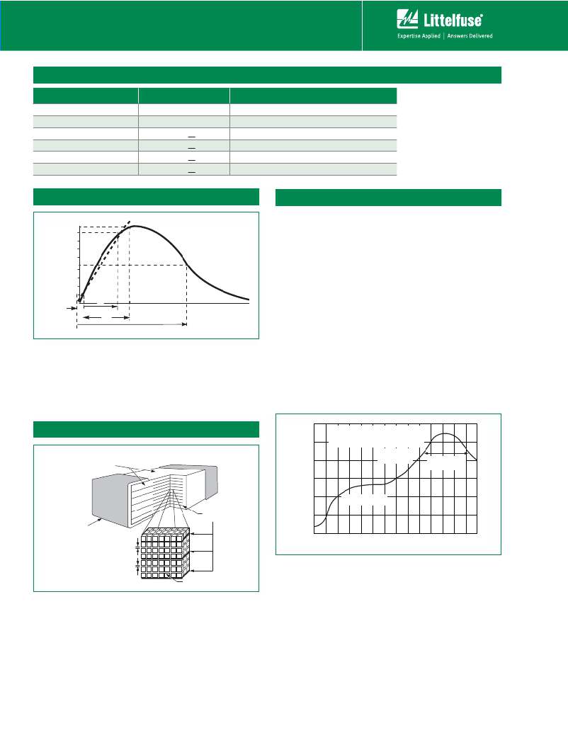
�Peak� Pulse� Current� Test� Waveform� for� Clamping� Voltage�
�100�
�50�
�Lead–free� (Pb-free)� Soldering� Recommendations�
�To� avoid� the� possibility� of� generating� stresses� due� to�
�thermal� shock,� a� preheat� stage� in� the� soldering� process�
�is� recommended,� and� the� peak� temperature� of� the� solder�
�process� should� be� rigidly� controlled.�
�When� using� a� re?ow� process,� care� should� be� taken� to�
�ensure� that� the� ML� chip� is� not� subjected� to� a� thermal�
�gradient� steeper� than� 4� degrees� per� second;� the� ideal�
�O� 1�
�0�
�T�
�TIME�
�gradient� being� 2� degrees� per� second.� During� the� soldering�
�process,� preheating� to� within� 100� degrees� of� the� solder's�
�T� 1�
�T� 2�
�0� 1� =� Virtual� Origin� of� Wave�
�T� =� Time� from� 10%� to� 90%� of� Peak�
�T� 1� =� Rise� Time� =� 1.25� x� T�
�T� 2� =� Decay� Time�
�Example� -� For� an� 8/20� μ� s� Current� Waveform:�
�8� μ� s� =� T� 1� =� Rise� Time�
�20� μ� s� =� T� 2� =� Decay� Time�
�peak� temperature� is� essential� to� minimize� thermal� shock.�
�Once� the� soldering� process� has� been� completed,� it� is�
�still� necessary� to� ensure� that� any� further� thermal� shocks�
�are� avoided.� One� possible� cause� of� thermal� shock� is� hot�
�printed� circuit� boards� being� removed� from� the� solder�
�process� and� subjected� to� cleaning� solvents� at� room�
�temperature.� The� boards� must� be� allowed� to� cool� gradually�
�to� less� than� 50o� C� before� cleaning.�
�Multilayer� Internal� Construction�
�300�
�250�
�MAXIMUM� TEMPERATURE� 260?C,�
�TIME� WITHIN� 5?C� OF� PEAK�
�20� SECONDS� MAXIMUM�
�RAMP� RATE�
�FIRED� CERAMIC�
�DIELECTRIC�
�200�
�<3?C/s�
�60� -� 150� SEC�
�>� 217?C�
�150�
�100�
�PREHEAT� ZONE�
�METAL� END�
�METAL�
�ELECTRODES�
�50�
�TERMINATION�
�0�
�0�
�1.0�
�2.0�
�3.0�
�4.0�
�5.0�
�6.0�
�7.0�
�DEPLETION�
�REGION�
�DEPLETION�
�REGION�
�GRAINS�
�TIME� (MINUTES)�
�0201� MLA� Varistor� Series�
�Revision:� June� 28,� 2010�
�?2010� Littelfuse,� Inc.�
�Speci?cations� are� subject� to� change� without� notice.�
�Please� refer� to� www.littelfuse.com/series/0201MLA.html� for� current� information.�
�发布紧急采购,3分钟左右您将得到回复。
相关PDF资料
V751NA34
VARISTR IND SQ DISC 750V 34MM NA
VA200060K121DL
VARISTOR TVS 60VDC 300A AXIAL
VAR-18120550M5P-XK
VARISTOR RING 55V 12MM 5-TERM
VC020116T150WP
VARISTOR TVS 16VDC 0201
VC06AG183R0YAT1A
VARISTOR 18VDC 3PF 0603
VC12LC18A500DP
VARISTOR TVS ESD 18VDC 30A 1206
VC15PA0160KBA
VARISTOR TVS ESD 16VDC1200A 2220
VCAC060322A470NRP
VARISTOR TVS 22VDC 30A 0603
相关代理商/技术参数
V5.5MLA0402
制造商:LITTELFUSE 制造商全称:Littelfuse 功能描述:Multilayer Transient Voltage Surge Suppressors
V5.5MLA0402LN
制造商:LITTELFUSE 制造商全称:Littelfuse 功能描述:Surface Mount Multilayer Varistors
V5.5MLA0402LNH
功能描述:压敏电阻 5.5V 20A 70pF
RoHS:否 制造商:EPCOS 产品:MLV 电压额定值 DC:22 V 电压额定值 AC:17 V 钳位电压:50 V 直径: 峰值浪涌电流:30 A 浪涌能量额定值:75 mJ 电容:74.2 pF 工作温度范围:- 55 C to + 125 C 安装:SMD/SMT 封装:Reel
V5.5MLA0402LNR
功能描述:压敏电阻 5.5V 20A 220pF 38V-CLAMP 15.9A-PK
RoHS:否 制造商:EPCOS 产品:MLV 电压额定值 DC:22 V 电压额定值 AC:17 V 钳位电压:50 V 直径: 峰值浪涌电流:30 A 浪涌能量额定值:75 mJ 电容:74.2 pF 工作温度范围:- 55 C to + 125 C 安装:SMD/SMT 封装:Reel
V5.5MLA0402LNR
制造商:Littelfuse 功能描述:Varistor 制造商:Littelfuse 功能描述:VARISTOR, 5.5V, 21V, 0402
V5.5MLA0402N
制造商:LITTELFUSE 制造商全称:Littelfuse 功能描述:Surface Mount Multilayer Varistors (MLVs)
V5.5MLA0402NH
功能描述:压敏电阻 5.5V 20A 220pF RoHS:否 制造商:EPCOS 产品:MLV 电压额定值 DC:22 V 电压额定值 AC:17 V 钳位电压:50 V 直径: 峰值浪涌电流:30 A 浪涌能量额定值:75 mJ 电容:74.2 pF 工作温度范围:- 55 C to + 125 C 安装:SMD/SMT 封装:Reel
V5.5MLA0402NR
功能描述:压敏电阻 5.5V 20A 220pF
RoHS:否 制造商:EPCOS 产品:MLV 电压额定值 DC:22 V 电压额定值 AC:17 V 钳位电压:50 V 直径: 峰值浪涌电流:30 A 浪涌能量额定值:75 mJ 电容:74.2 pF 工作温度范围:- 55 C to + 125 C 安装:SMD/SMT 封装:Reel